Intel Says It’ll Deliver 2025 Chip Tech a Half Year Early
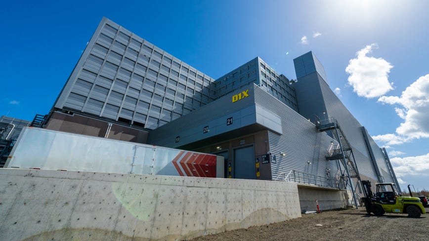
Intel has expanded its D1X fab in Oregon with Mod3, a building with 270,000 new square feet for the biggest new chipmaking machines.
Intel
After years of trouble and delay, Intel’s chipmaking business finally has some good news to report. The most advanced manufacturing process the company has committed to will arrive in the second half of 2024, six months earlier than planned.
Intel fell behind rivals Taiwan Semiconductor Manufacturing Co. (TSMC) and Samsung because of problems modernizing its manufacturing, and it convinced chip designer Pat Gelsinger to return to the company as chief executive in 2021. Shortly afterward, Intel laid out a road map that meant five improvements to its manufacturing processes in four years, with manufacturing processes named Intel 7, Intel 4, Intel 8, Intel 20A and Intel 18A. Each step improves a chip’s performance relative to its power consumption.
Those steps are the foundation of a plan to catch up to rivals in 2024 and surpass them in 2025. If successful, Gelsinger’s plan will help Windows PCs keep up with ever more powerful Macs, return Intel to its glory days at the vanguard of the semiconductor business, justify its tens of billions of dollars of expenditures and slow the shift of chip manufacturing from the US to Asia.
“Intel must have good confidence in the [schedule] pull in,” said Tirias analyst Kevin Krewell. “Otherwise, why announce it this early?”
Chip challenges
- Intel Buys the Industry’s First Next-gen Chipmaking Tool To Try To Reclaim Lead
- Apple’s M1 Ultra Shows the Future of Computer Chips
- What It’s Like Inside a $7 Billion Intel Fab
- Intel’s Chip Recovery Plan Could Restore US Manufacturing Prowess
Intel detailed the advancement along with the announcement that it’s opened its latest chip fabrication facility, or fab, devoted to developing its next-gen manufacturing processes. It performs such work at its newly named Gordon Moore Park in Oregon, where it’s investing $3 billion in the new Mod3 wing of its D1X fab. Intel replicates its D1X processes across fabs all around the world.
The manufacturing progress news bodes well not just for Intel’s 2024 chips, but also for Intel’s business using the steps on the way.
Those steps are important for Intel’s own processors and for another part of Gelsinger’s recovery plan, Intel Foundry Services, a separate business unit set up to build others’ chips the way TSMC and Samsung do. IFS customers will get access to Intel 3 and Intel 18A processes, the company said.
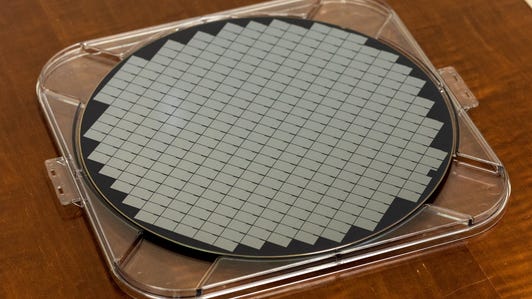
Gelsinger had hinted earlier that its chip manufacturing improvements were on or ahead of schedule, and he showed off an 18A wafer with test chips in February. Intel didn’t offer specifics on what went well.?
The new 270,000-square-foot Mod3 building has high enough ceilings and strong enough floors to accommodate the latest machines used to etch circuitry onto the silicon crystal wafers that after months of processing steps become microchips, said Ryan Russell, corporate vice president of logic technology development.
Intel was slower than rivals to move to chipmaking equipment that uses extreme ultraviolet light to inscribe smaller circuitry elements on chips, a technology called photolithography that’s a key part of processor miniaturization. Under Gelsinger, Intel is trying to play nicer with chip fabrication equipment makers like Dutch ASML. Indeed, Intel will receive ASML’s first model of a second generation of EUV machines using an approach called high numeric aperture that inscribes finer lines than conventional EUV.
Intel has taken several measures to ensure it doesn’t repeat mistakes made adopting its last two manufacturing processes, called Intel 10 and Intel 7. For one thing, it’s spending more money on test wafers to try different options.
“Having more silicon that you can run in parallel really lets you speed up your development process because you can afford to run more innovative experiments,” Russell said.
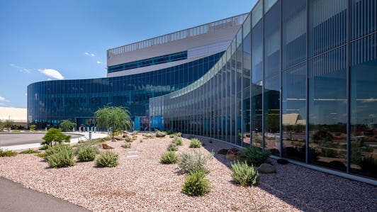
A look inside Intel’s mammoth Arizona chipmaking fab
For another, Intel has decoupled improvements and developed contingency plans so it can keep moving ahead even if all its ideas don’t pan out.
Two big developments coming with Intel 20A are backside power delivery, branded PowerVia, which moves electrical power supply circuitry to the opposite side of the processor instead of blending it with millions of communication channels. Another is the new “gate all around” design for transistors, the core circuitry element that processes data, which Intel brands as RibbonFET.
They’re both dramatic changes, but Intel is developing PowerVia with conventional transistors, too, in case the RibbonFET approach has problems, said Sanjay Natarajan, senior vice president of logic technology development.
Intel also is adopting high numeric aperture lithography more flexibly. That’s scheduled to arrive in Intel’s 2025 chipmaking process, but the company can change course.
“We’re prepared for a 2025 intercept,” Natarajan said. “If high NA is really mature later, let’s say 2026, we’re prepared for the right intercepts there.”